- 您现在的位置:买卖IC网 > Sheet目录1995 > HI5760BIBZ (Intersil)CONV D/A 10-BIT 125MSPS 28-SOIC
16
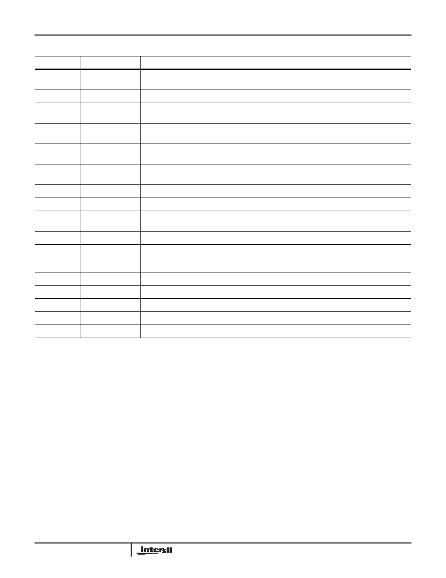
Pin Descriptions
PIN NO.
PIN NAME
PIN DESCRIPTION
1-10
D9 (MSB) Through
D0 (LSB)
Digital Data Bit 9 (Most Significant Bit) through Digital Data Bit 0, (Least Significant Bit).
11-14
NC
No Connect. Recommend ground.
15
SLEEP
Control Pin for Power-Down mode. Sleep Mode is active high; Connect to ground for Normal Mode. Sleep
pin has internal 20
A active pulldown current.
16
REFLO
Connect to analog ground to enable internal 1.2V reference or connect to AVDD to disable internal
reference.
17
REFIO
Reference voltage input if internal reference is disabled. Reference voltage output if internal reference is
enabled. Use 0.1
F cap to ground when internal reference is enabled.
18
FSADJ
Full Scale Current Adjust. Use a resistor to ground to adjust full scale output current. Full Scale Output
Current = 32 x VFSADJ/RSET.
19
COMP1
For use in reducing bandwidth/noise. Recommended: connect 0.1
F to AV
DD .
20
ACOM
Analog Ground.
21
IOUTB
The complimentary current output of the device. Full scale output current is achieved when all input bits
are set to binary 0.
22
IOUTA
Current output of the device. Full scale output current is achieved when all input bits are set to binary 1.
23
NC
Internally connected to ACOM via a resistor. Recommend leave disconnected. Adding a capacitor to
ACOM for upward compatibility is valid. Grounding to ACOM is valid. (For upward compatibility to 12-bit
and 14-bit devices, pin 23 needs the ability to have a 0.1
F capacitor to ACOM.)
24
AVDD
Analog Supply (+3V to +5V).
25
NC
No Connect. (For upward compatibility to 12 and 14b devices, pin 25 needs to be grounded to ACOM.)
26
DCOM
Digital Ground.
27
DVDD
Digital Supply (+3V to +5V).
28
CLK
Input for clock. Positive edge of clock latches data.
HI5760
发布紧急采购,3分钟左右您将得到回复。
相关PDF资料
HI5762/6IN
CONV A/DDUAL 10BIT 60MSPS 44MQFP
HI5766KCB
CONV A/D 10BIT 60MSPS 28-SOIC
HI5767/6IB
CONV A/D 10BIT 60MSPS 28-SOIC
HI5805BIB
IC ADC 12-BIT 5MSPS 28-SOIC
HI5812JIBZ-T
ADC 12BIT SAMPL TRK&HOLD 24-SOIC
HI5828IN
DAC DUAL 12BIT 130MHZ 48-LQFP
HI5860IBZ
CONV D/A 12-BIT 130MSPS 28-SOIC
HI5960IAZ
CONV D/A 14BIT 130MSPS 28-TSSOP
相关代理商/技术参数
HI5760BIBZ-T
功能描述:数模转换器- DAC D/A 10-BIT 125MSPS 28PIN INDUST TEMP RoHS:否 制造商:Texas Instruments 转换器数量:1 DAC 输出端数量:1 转换速率:2 MSPs 分辨率:16 bit 接口类型:QSPI, SPI, Serial (3-Wire, Microwire) 稳定时间:1 us 最大工作温度:+ 85 C 安装风格:SMD/SMT 封装 / 箱体:SOIC-14 封装:Tube
HI5760EVAL1
功能描述:数据转换 IC 开发工具 HI5760 EVAL PL ATFORM PKG
RoHS:否 制造商:Texas Instruments 产品:Demonstration Kits 类型:ADC 工具用于评估:ADS130E08 接口类型:SPI 工作电源电压:- 6 V to + 6 V
HI5760EVALI
制造商:Harris Corporation 功能描述:
HI5760IA
功能描述:CONV D/A 10-BIT 125MSPS 28-TSSOP RoHS:否 类别:集成电路 (IC) >> 数据采集 - 数模转换器 系列:- 标准包装:2,400 系列:- 设置时间:- 位数:18 数据接口:串行 转换器数目:3 电压电源:模拟和数字 功率耗散(最大):- 工作温度:-40°C ~ 85°C 安装类型:表面贴装 封装/外壳:36-TFBGA 供应商设备封装:36-TFBGA 包装:带卷 (TR) 输出数目和类型:* 采样率(每秒):*
HI5760IA-T
功能描述:CONV D/A 10-BIT 125MSPS 28-TSSOP RoHS:否 类别:集成电路 (IC) >> 数据采集 - 数模转换器 系列:- 标准包装:2,400 系列:- 设置时间:- 位数:18 数据接口:串行 转换器数目:3 电压电源:模拟和数字 功率耗散(最大):- 工作温度:-40°C ~ 85°C 安装类型:表面贴装 封装/外壳:36-TFBGA 供应商设备封装:36-TFBGA 包装:带卷 (TR) 输出数目和类型:* 采样率(每秒):*
HI5760IAZ
功能描述:数模转换器- DAC D/A 10-BIT 125MSPS 28PIN INDUST TEMP RoHS:否 制造商:Texas Instruments 转换器数量:1 DAC 输出端数量:1 转换速率:2 MSPs 分辨率:16 bit 接口类型:QSPI, SPI, Serial (3-Wire, Microwire) 稳定时间:1 us 最大工作温度:+ 85 C 安装风格:SMD/SMT 封装 / 箱体:SOIC-14 封装:Tube
HI5760IAZ-T
功能描述:数模转换器- DAC D/A 10-BIT 125MSPS 28PIN INDUST TEMP RoHS:否 制造商:Texas Instruments 转换器数量:1 DAC 输出端数量:1 转换速率:2 MSPs 分辨率:16 bit 接口类型:QSPI, SPI, Serial (3-Wire, Microwire) 稳定时间:1 us 最大工作温度:+ 85 C 安装风格:SMD/SMT 封装 / 箱体:SOIC-14 封装:Tube
HI5762
制造商:INTERSIL 制造商全称:Intersil Corporation 功能描述:Dual 10-Bit, 60MSPS A/D Converter with Internal Voltage Reference